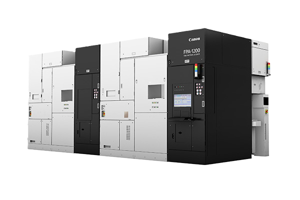
Canon said its latest machine, called the FPA-1200NZ2C, will be able to make semiconductors equivalent to a 5nm process and go as small as 2nm. For context, the A17 Pro chip inside Apple’s iPhone 15 Pro and Pro Max, is a 3nm semiconductor.
Both TSMC and South Korea’s Samsung, the two biggest advanced chip manufacturing companies, are aiming to make 2nm chips in 2025.
Lithography machines are key to effectively print the design of a chip onto the material that ends up going into the semiconductor.
ASML’s machines use ultraviolet light during that process. Canon said its machine does not require a light source with a special wavelength, therefore reducing power consumption.
Canon’s traditional strength in cameras, optical equipment and printers, has seen it renew its focus on the semiconductor supply chain at a time when the world is increasingly in need of chips to power technologies like artificial intelligence.
Arjun Kharpal
Interesting business decision by Canon to enter the semiconductor manufacturing market at a time when chips are both highly sought after and highly contentions because of the US sanctions against China. Further reporting states that their machines should be considerably cheaper, up to ten times, than ASML’s EUV lithography systems, which would make them attractive to smaller fabs or startups that can’t afford to spend around $200 million for one piece of equipment.

I have always considered that Canon maintained an important strategic advantage over Nikon because it designs and manufactures its own chips, as opposed to Nikon, who relies on Sony for manufacturing. Even though Sony was making rapid advances in camera chips and mirrorless technology, Canon has managed to catch up and now competes with Sony on a roughly equal footing, whereas Nikon is lagging behind in focusing performance. Making this manufacturing equipment available for external customers serves to demonstrate Canon’s advantage, and could improve its business considerably if the machines live up to expectations.
Post a Comment